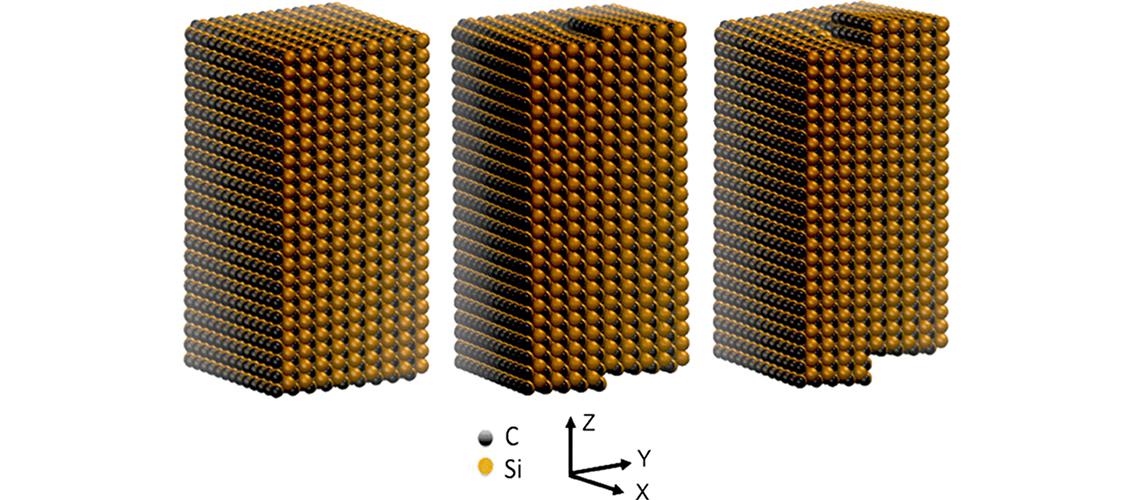
Materials whose atoms form a crystal structure - the atoms are organized in a symmetric spatial arrangement - are useful for various applications, such as electronics. During the crystal growth process, dislocations can form. One type is called a “screw dislocation,” which can be seen in the image above. Defects in a crystal will affect its properties and thus have implications for the material’s use.
MSI Principal Investigator Traian Dumitrica, an associate professor in the Department of Mechanical Engineering (College of Science and Engineering), post-doctoral fellow Dr. Yuxiang Ni, and their colleagues at the Ecole Centrale Paris have been studying screw dislocations by performing equilibrium molecular dynamics simulations on MSI’s supercomputers. In a recent paper, these researchers discussed their finding that the area around a screw dislocation in a silicon carbide crystal has higher internal thermal resistance than the rest of the material. This is interesting theoretically, and the findings also can be applied to the design of materials useful for high-temperature electronics and thermoelectric applications. The paper was featured on the cover of the prestigious journal Physical Review Letters in September 2014. (Y Ni, S. Xiong, S. Volz, T. Dumitrica. Thermal transport along the dislocation line in silicon carbide. 2014. Physical Review Letters. 113, 124301).
Professor Dumitrica and his research group use MSI resources for molecular dynamics simulations related to studies of the mechanical properties, stability, and behavior of nanoscale materials. A previous paper was featured in a Research Spotlight, “Modeling Properties of Graphene,” in August 2014.
Image description: Supercells for the SiC calculations: pristine (left), 1b (center) and 2b (right) screw dislocated (b = 3.08 Å). The heat carrying direction is z. The cross-section dimensions are 4 x 4 nm. Length is 7 nm. Image and description Ni, Y et al., PRL, 2014, 113:124301. ©2014 American Physical Society
posted on March 18, 2015